Animated Text
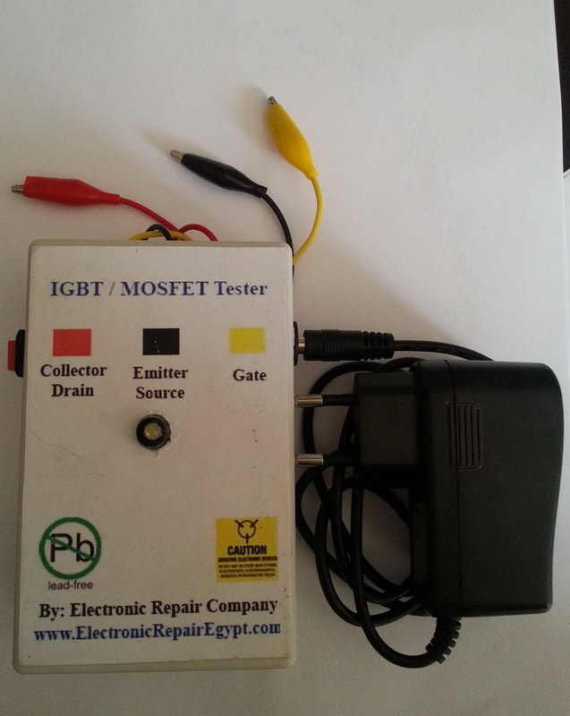
Looking for a premium IGBT and Mosfet tester to troubleshoot and repair your power inverters, UPS systems, PSU units, or plasma cutters? Electronic Repair Company Egypt's IGBT and Mosfet tester is the perfect solution! Our high-quality, hand-made functional tester is designed to provide accurate diagnostics and testing, ensuring that your repairs are done right the first time. Whether you're a professional technician or a DIY enthusiast, our IGBT tester is a must-have tool in your arsenal.
Trust in the quality and reliability of Electronic Repair Company Egypt's IGBT and Mosfet tester for all your electrical repair needs. Order now and experience the difference!"
Trust in the quality and reliability of Electronic Repair Company Egypt's IGBT and Mosfet tester for all your electrical repair needs. Order now and experience the difference!"
High Quality Components - High Accuracy - Functional Test - Accurate - Handmade Tester
|
|
The best MOSFET Tester IGBT Tester 2
|
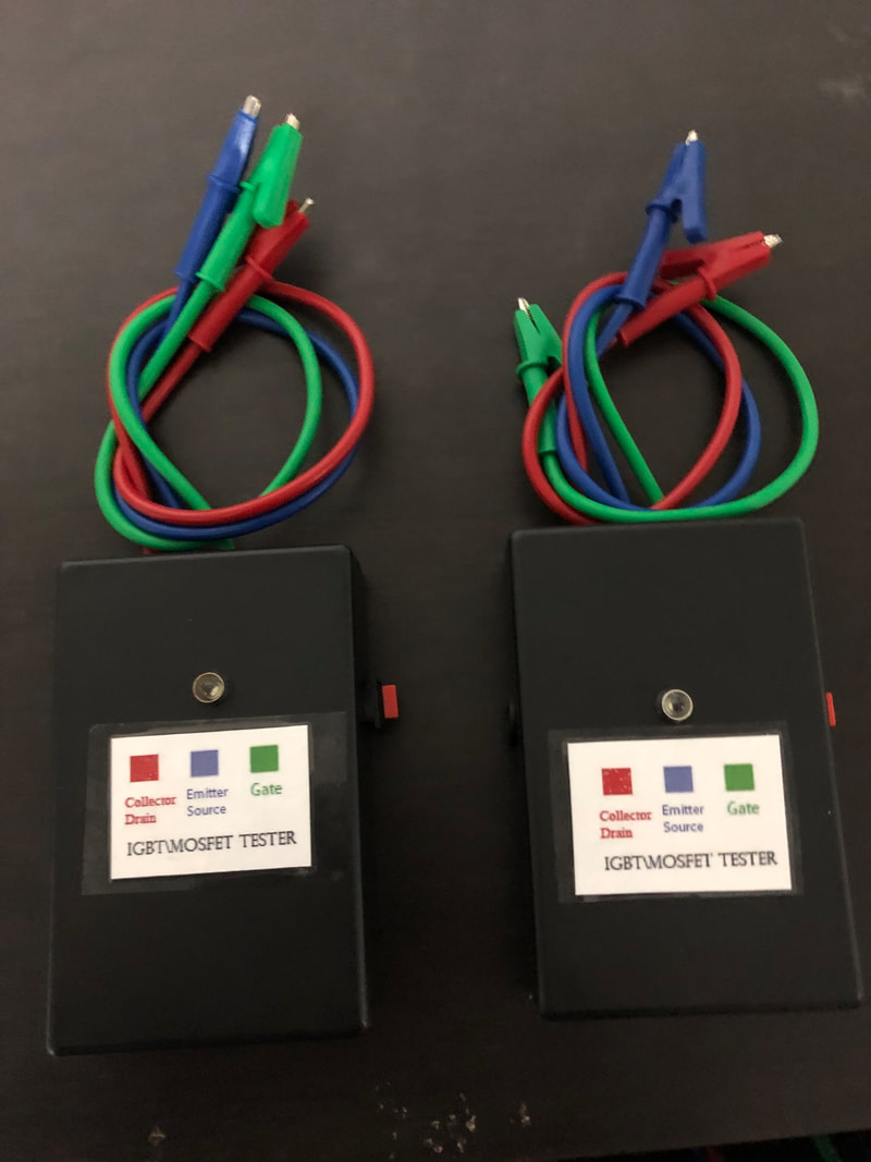
The best MOSFET Tester IGBT Tester 1
|
|
Test Techniques:
applying a very small current to Gate of the component. a small electrostatic field causes conduction between Collector / Emitter junction In case of IGBT & In case of MOSFET , Drain / Source junction
can used with all types and Diode protection Mosfets and IGBTs
applying a very small current to Gate of the component. a small electrostatic field causes conduction between Collector / Emitter junction In case of IGBT & In case of MOSFET , Drain / Source junction
can used with all types and Diode protection Mosfets and IGBTs
|
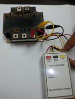
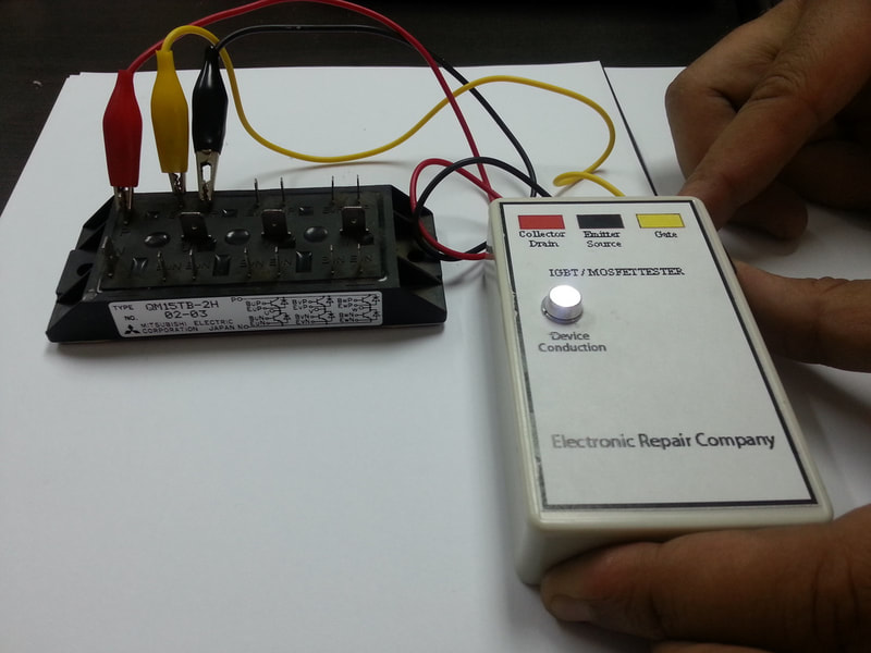
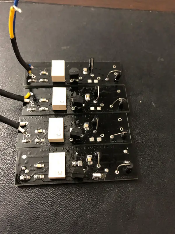
Product Application: This Test Equipment would typically be used for Functional Test and Repair of products utilizing Switch Mode (switching) Power Supplies, Inverters or Chopper circuits. Some product examples are 115/ 230V Power Inverters, UPS Battery backup units (Uninterruptible PSU), Inverter based Welders, and Plasma Cutters. |
The switching circuits in these products characteristically use either IGBT's or MOSFET's. The choice of which component is used is governed by the switching speed, current capacity and breakdown voltage requirements of the design. It is important to note that these components are typically N-channel devices that require a positive gate voltage. MOSFET's should be enhancement-mode devices (normally off). Depletion mode devices are less common in these products. |
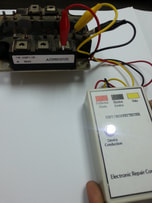
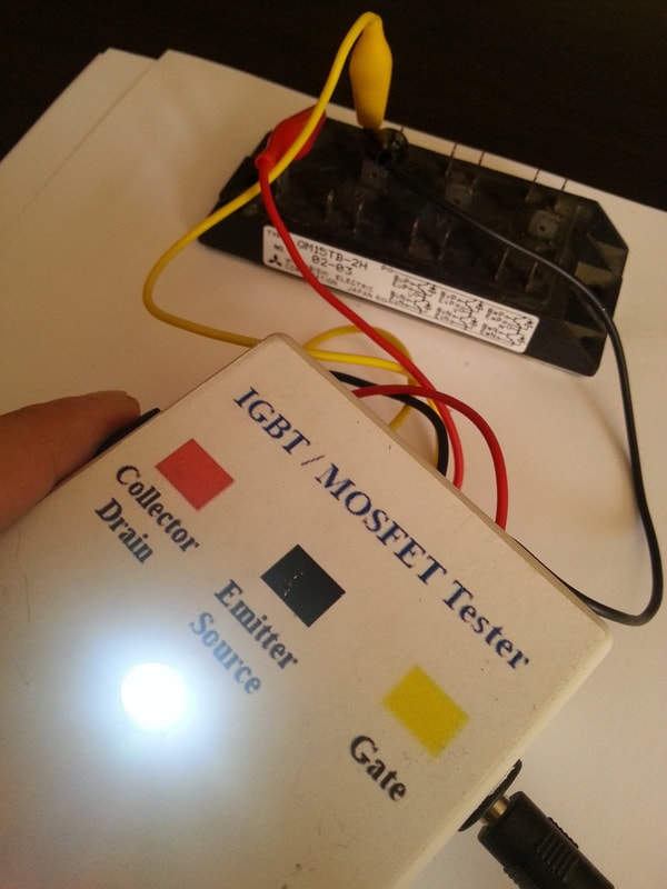
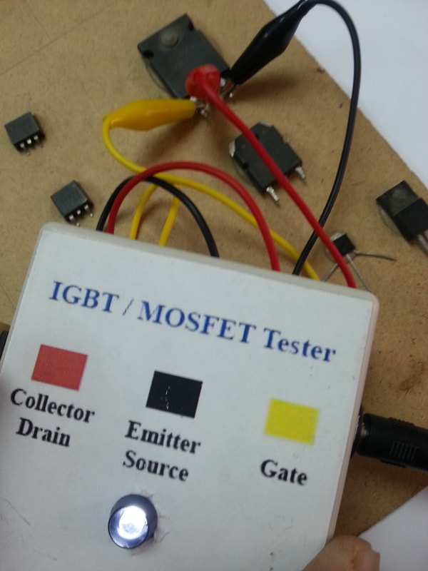
By pressing the Test button on the IGBT & MOSFET Tester you apply a very small current to the Gate of the component. The voltage associated with this causes an electrostatic field to be setup within the Gate junction of the component. This small field causes conduction to take place in the Collector / Emitter junction (in an IGBT) or Drain / Source junction (in a MOSFET). The status of the component is displayed on the Device Conduction LED.
MOSFET IGBT Tester 1
|
MOSFET IGBT Tester 2
|
MOSFET IGBT Tester 3
|
MOSFET IGBT Tester 4
|
MOSFET IGBT Tester 5
|
|
IGBT's (Insulated Gate Bipolar Transistor)
MOSFET's (Metal Oxide Semiconductor Field Effect Transistor) Simple, Any One can use it |
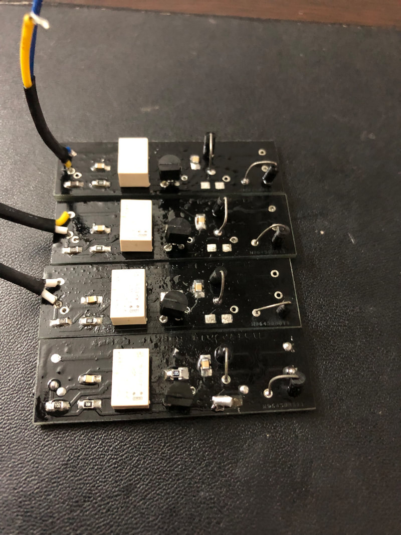
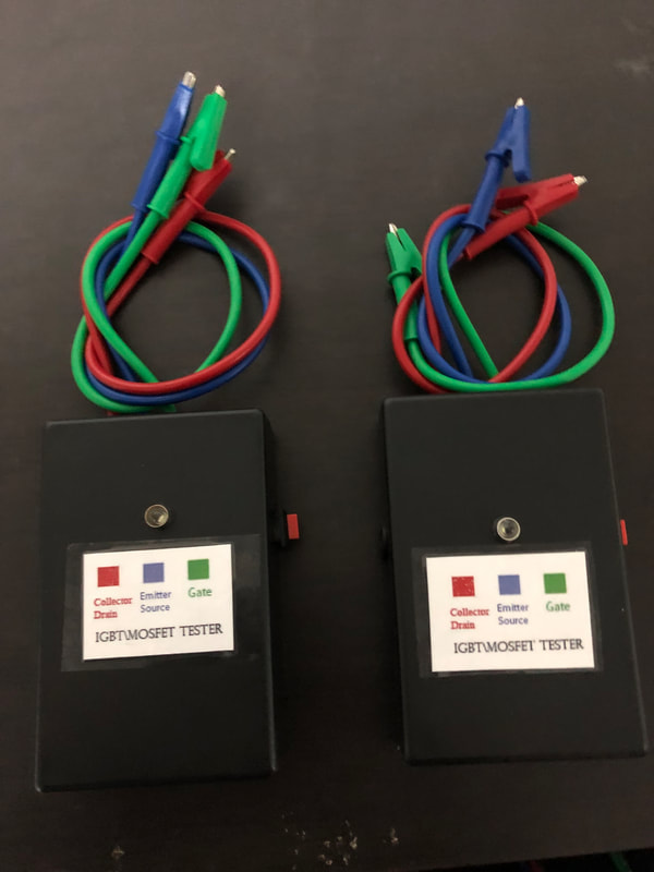
Specifications • Single button Testing of IGBT's and MOSFET's, including the Reverse Bias condition of Protection Diodes. • Active gate current limited to 8mA for device protection. • Collector/Drain switching current limited to 22mA. • ESD protection of the Device-Under-Test (during off time). The Gate to Emitter/Source potential is limited to 0 VDC. • Light, easy to handle enclosure. • 24" Test Leads with Alligator clips (Red, Black and Yellow). • PCB based design with a hybrid architecture utilizing SMT, and Through Hole components. |
Test Steps:
JUST CONNECT THE TEST LEADS
PRESS TEST BUTTON
If the LED lights, you have a Good functional device
The best MOSFET Tester IGBT Tester 3
|
The best MOSFET Tester IGBT Tester 4
|
The best MOSFET Tester IGBT Tester 5
|
We will activate the TECHNICAL SUPPORT PAGE, Once you will recive your package